On Friday, Elon Musk posted this:
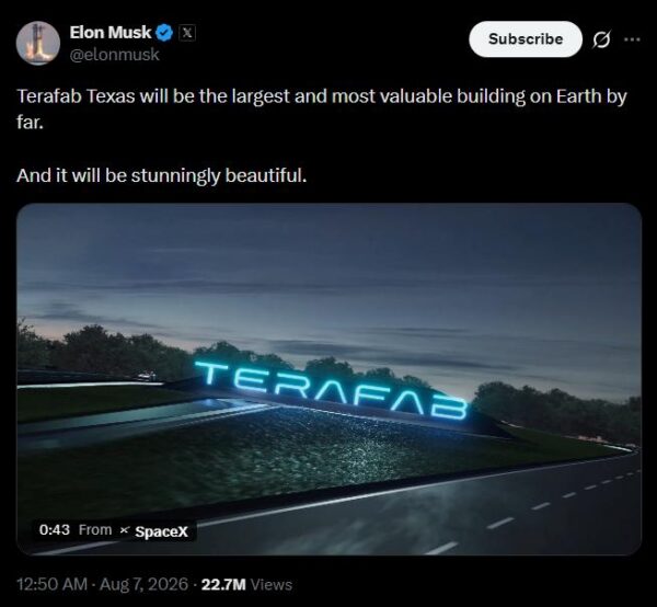
It was a video of the night time rendering and aerial shots of Terafab, the chip plant it is building in Grimes County, Texas.
Here’s another snapshot of the aerial mock up…

Most people looked at the building, and fair enough.
It will run 2.5 miles end to end, with more than 100 million square feet of floor space under one unbroken roof.
If it gets finished, it will be the largest building on Earth.
But when you really look at that image, what do you see?
I’ll tell you what I see.
I see a ring.
A ring that is so large in scale it reminds me a heck of a lot of this:
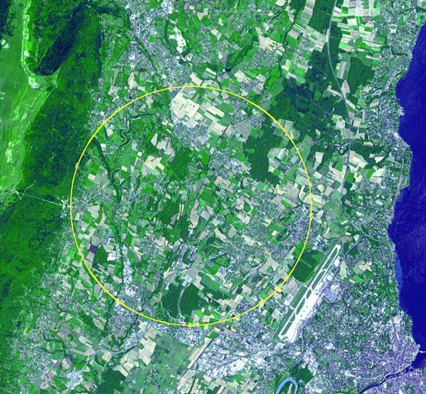 Source: NASA
This ring is the Large Hadron Collider in Switzerland.
Note: You can’t actually see this ring from the sky, but it’s under there, and it’s massive.
Elon isn’t building his own particle accelerator at Terafab… is he?
Surely not.
As soon as this went onto X, the speculation began. And all weekend, it accelerated (so to speak).
Is there a particle accelerator under there?
Is Elon building CERN 2.0?
Didn’t Elon originally want to work at CERN?
Then speculation began that it was indeed a synchrotron and that Elon was actually building a free electron laser (FEL).
Musk replied,
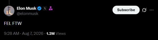
“Free electron laser, for the win.”
Britain’s Investment Letter Since 1938
In 1938, The Fleet Street Letter warned its readers that war was coming to Europe — and even identified September as the critical month.
Since then, its readers have been warned ahead of Black Monday, the dotcom crash and the 2008 financial crisis.
Today, Britain’s longest-running investment advisory is still looking for the “news behind the news” — and the investment opportunities others could be missing.
Click here to discover what The Fleet Street Letter sees coming next.
Capital at risk.
What Does Britain’s Oldest Investment Letter See Coming Next?
It warned readers ahead of Black Monday.
The dotcom crash.
And the 2008 financial crisis.
Now, nearly 90 years after it was founded, The Fleet Street Letter is still searching for the “news behind the news” — and the investment opportunities that could emerge from the next major turning point.
Click here to discover what its editors are seeing now.
Capital at risk.
What the ring does
Every advanced chip in your phone, your car, and every AI server on the planet gets printed using extreme ultraviolet light, or EUV.
One company makes the machines that do it, ASML (Nasdaq: ASML), and they cost hundreds of millions of dollars each.
The way ASML makes it all sounds like pure wizardry.
A carbon dioxide laser fires at droplets of molten tin about 50,000 times a second. Each droplet gets hit twice.
The first hit flattens it into a disc, and the second blasts it into plasma hot enough to throw off EUV as a by-product.
It works. No one else in the world can figure out how, but it built the entire modern chip industry and AI rollout as we know it.
It is also wasteful, messy with tin debris, and every scanner needs its own source bolted to it…
A free-electron laser achieves the same outcome, but in a different way.
You accelerate electrons to near light speed, then run them through a line of magnets that make them wiggle. The wiggling throws off light.
Change the magnets and you change the wavelength, and there is no tin and no debris.
One accelerator can also feed a lot of scanners at once.
xLight, the Palo Alto startup furthest down the FEL road, reckons a single FEL could supply as many as 20 ASML scanners at four times the power.
One FEL as a central light utility for the whole building, instead of every scanner carrying its own tin-droplet source.
That is where the money is, because the light source is roughly half the cost of an EUV machine…
Power at the source caps how many wafers an hour a fab can push out, so more light at Terafab is simply more chips.
If Terafab’s free-electron laser works as hoped, where could the biggest economic advantage come from?
|
Bigger than rockets
Musk has landed rockets on barges and put thousands of satellites into orbit, turned the car market on its head, redefined the social media landscape, helped push AI into the mainstream, and developed autonomous digging machines to make new transportation links.
Of all the things he’s done (like him or loathe him), Terafab may end up as the biggest and most valuable of them all.
Phase one of Terafab costs US$16.8 billion, and the full buildout runs to US$119 billion.
The 3,000 jobs announced last week cover only the first of 10 planned phases.
This facility will house the manufacturing, packaging and testing of advanced logic and memory devices.
Nobody does all three under one roof.
TSMC, Samsung, and the packaging houses are spread across companies and continents.
The target at Tearfab is more than one terawatt of compute a year.
Now add building his own light source to that list.
And then the ability to build everything from logic to memory.
The potential value of that quite likely exceeds the current value of SpaceX and Tesla combined.
It looks to me like the most ambitious at least (believe it or not, which is saying something considering his view to colonise Mars!)
Intel (Nasdaq: INTC) signed on in April to help design, fabricate, and package for Terafab, the first outside commitment its foundry arm has ever won.
And while this is seen as a potential threat to something like ASML, it does not get killed by this either. An FEL replaces the light source, not the scanner.
Therefore, it’s no great surprise to know ASML’s chief executive has confirmed direct talks with Musk about the project.
So watch for one thing over the next six months.
Does Terafab name an FEL partner? Does Elon get more public than just “FEL FTW?”
If yes to both, that means Intel and ASML are seemingly already inside the door here and that would be a massive tailwind for both.
Also, it would seem like the pace of acceleration in AI hardware fabrication is about to get a massive kick up the backside, and for investors in the AI rollout, that’s a good thing too.
Until next time,
Sam Volkering
Investment Director, Southbank Investment Research
PS Whether Musk really is planning to put a free-electron laser inside Terafab remains to be seen. But if he is, it’s another reminder of just how quickly the AI investment story is evolving. Six months from now, the companies making the biggest money from this boom may not be the ones everyone is watching today. That’s why having Jim, Nick, and James looking at the market from three very different angles could prove so valuable. You can find out how to put all three to work for you here.